Saturday 27 November 2010

Graphene Potential applications

Disusun Ulang Oleh:

Arip Nurahman
Department of Physics
Faculty of Sciences and Mathematics, Indonesia University of Education

and

Follower Open Course Ware at Massachusetts Institute of Technology
Cambridge, USA

Department of Physics
http://web.mit.edu/physics/
http://ocw.mit.edu/OcwWeb/Physics/index.htm

&

Aeronautics and Astronautics Engineering
http://web.mit.edu/aeroastro/www/
http://ocw.mit.edu/OcwWeb/Aeronautics-and-Astronautics/index.htm


Potential applications


Single-molecule gas detection


Theoretically graphene makes an excellent sensor due to its 2D structure. The fact that its entire volume is exposed to its surrounding makes it very efficient to detect adsorbed molecules. However, similar to carbon nanotubes, graphene has no dangling bonds on its surface. Gaseous molecules cannot be readily adsorbed onto graphene surface. So intrinsically graphene is insensitive. The sensitivity of graphene chemical gas sensors can be dramatically enhanced by functionalizing graphene, for example, coating with a thin layer of certain polymers. The thin polymer layer acts like a concentrator that absorbs gaseous molecules. The molecule absorption introduces a local change in electrical resistance of graphene sensors. While this effect occurs in other materials, graphene is superior due to its high electrical conductivity (even when few carriers are present) and low noise which makes this change in resistance detectable.

Graphene nanoribbons


Graphene nanoribbons (GNRs) are essentially single layers of graphene that are cut in a particular pattern to give it certain electrical properties. Depending on how the un-bonded edges are configured, they can either be in a zigzag or armchair configuration. Calculations based on tight binding predict that zigzag GNRs are always metallic while armchairs can be either metallic or semiconducting, depending on their width. 

However, recent density functional theory calculations show that armchair nanoribbons are semiconducting with an energy gap scaling with the inverse of the GNR width. Indeed, experimental results show that the energy gaps do increase with decreasing GNR width. However, as of February 2008, no experimental results have measured the energy gap of a GNR and identified the exact edge structure. Zigzag nanoribbons are also semiconducting and present spin-polarized edges. 

Their 2D structure, high electrical and thermal conductivity, and low noise also make GNRs a possible alternative to copper for integrated circuit interconnects. Some research is also being done to create quantum dots by changing the width of GNRs at select points along the ribbon, creating quantum confinement.

Graphene transistors


Due to its high electronic quality, graphene has also attracted the interest of technologists who see it as a way of constructing ballistic transistors. Graphene exhibits a pronounced response to perpendicular external electric fields, allowing one to build FETs (field-effect transistors). In their 2004 paper, the Manchester group demonstrated FETs with a "rather modest" on-off ratio of ~30 at room temperature. In 2006, Georgia Tech researchers, led by Walter de Heer, announced that they had successfully built an all-graphene planar FET with side gates. Their devices showed changes of 2% at cryogenic temperatures. 

The first top-gated FET (on-off ratio of <2) was demonstrated by researchers of AMICA and RWTH Aachen University in 2007. Graphene nanoribbons may prove generally capable of replacing silicon as a semiconductor in modern technology.

Facing the fact that current graphene transistors show a very poor on-off ratio, researchers are trying to find ways for improvement. In 2008, researchers of AMICA and University of Manchester demonstrated a new switching effect in graphene field-effect devices. This switching effect is based on a reversible chemical modification of the graphene layer and gives an on-off ratio of greater than six orders of magnitude. These reversible switches could potentially be applied to nonvolatile memories.

In 2009, researchers at the Politecnico di Milano demonstrated four different types of logic gates, each composed of a single graphene transistor. In the same year, the Massachusetts Institute of Technology researchers built an experimental graphene chip known as a frequency multiplier. It is capable of taking an incoming electrical signal of a certain frequency and producing an output signal that is a multiple of that frequency. Although these graphene chips open up a range of new applications, their practical use is limited by a very small voltage gain (typically, the amplitude of the output signal is about 40 times less than that of the input signal). Moreover, none of these circuits was demonstrated to operate at frequencies higher than 25 kHz.

In February 2010, researchers at IBM reported that they have been able to create graphene transistors with an on and off rate of 100 gigahertz, far exceeding the rates of previous attempts, and exceeding the speed of silicon transistors with an equal gate length. The 240 nm graphene transistors made at IBM were made using extant silicon-manufacturing equipment, meaning that for the first time graphene transistors are a conceivable—though still fanciful—replacement for silicon.

Graphene optical modulators


When the Fermi level of graphene is tuned, the optical absorption of graphene can be changed. In 2011, researchers at UC Berkeley reported the first graphene-based optical modulator. Operating at 1.2 GHz without any temperature controller, this modulator has a broad bandwidth (from 1.3 to 1.6 μm) and small footprint (~25 μm2).

Integrated circuits


Graphene has the ideal properties to be an excellent component of integrated circuits. Graphene has a high carrier mobility, as well as low noise, allowing it to be used as the channel in a FET. The issue is that single sheets of graphene are hard to produce, and even harder to make on top of an appropriate substrate. Researchers are looking into methods of transferring single graphene sheets from their source of origin (mechanical exfoliation on SiO2 / Si or thermal graphitization of a SiC surface) onto a target substrate of interest.[141]
In 2008, the smallest transistor so far, one atom thick, 10 atoms wide was made of graphene.[142] IBM announced in December 2008 that they fabricated and characterized graphene transistors operating at GHz frequencies.[143] In May 2009, an n-type transistor was announced meaning that both n and p-type transistors have now been created with graphene.[144] A functional graphene integrated circuit was also demonstrated – a complementary inverter consisting of one p- and one n-type graphene transistor.[145]
However, this inverter also suffered from a very low voltage gain.

According to a January 2010 report,[146] graphene was epitaxially grown on SiC in a quantity and with quality suitable for mass production of integrated circuits. At high temperatures, the Quantum Hall effect could be measured in these samples. See also the 2010 work by IBM in the transistor section above in which they made 'processors' of fast transistors on 2-inch (51 mm) graphene sheets.[137][138]

In June 2011, IBM researchers announced[147] that they had succeeded in creating the first graphene-based integrated circuit, a broadband radio mixer. The circuit handled frequencies up to 10 GHz, and its performance was unaffected by temperatures up to 127 degrees Celsius.


Electrochromic devices


Graphene oxide can be reversibly reduced and oxidized using electrical stimulus. Controlled reduction and oxidation in two-terminal devices containing multilayer graphene oxide films are shown to result in switching between partially reduced graphene oxide and graphene, a process which modifies the electronic and optical properties. Oxidation and reduction are also shown to be related to resistive switching. [148] [149]

Transparent conducting electrodes


Graphene's high electrical conductivity and high optical transparency make it a candidate for transparent conducting electrodes, required for such applications as touchscreens, liquid crystal displays, organic photovoltaic cells, and organic light-emitting diodes. In particular, graphene's mechanical strength and flexibility are advantageous compared to indium tin oxide, which is brittle, and graphene films may be deposited from solution over large areas.[150][151]

Large-area, continuous, transparent, and highly conducting few-layered graphene films were produced by chemical vapor deposition and used as anodes for application in photovoltaic devices. A power conversion efficiency (PCE) up to 1.71% was demonstrated, which is 55.2% of the PCE of a control device based on indium-tin-oxide.[152]


Organic light-emitting diodes (OLEDs) with graphene anodes have also been demonstrated.[153] The electronic and optical performance of devices based on graphene are shown to be similar to devices made with indium-tin-oxide.


An all carbon-based device called a light-emitting electrochemical cell (LEC) was demonstrated with chemically derived graphene as the cathode and the conductive polymer PEDOT as the anode by Matyba et al.[154] Unlike its predecessors, this device contains no metal, but only carbon-based electrodes. The use of graphene as the anode in LECs was also verified in the same publication.

Reference material for characterizing electroconductive and transparent materials


One layer of graphene absorbs 2.3 % of white light.[155] This property was used to define the Conductivity of Transparency that combines the sheet resistance and the transparency. This parameter was used to compare different materials without the use of two independent parameters.[156]

Thermal management materials-Thermal interfacial materials


In 2011, researchers in Georgia Institute of Technology reported that a three-dimensional vertically aligned functionalized multilayer graphene architecture can be an approach for graphene-based thermal interfacial materials (TIMs) with superior equivalent thermal conductivity and ultra-low interfacial thermal resistance between graphene and metal.[157]

Solar cells


The USC Viterbi School of Engineering lab reported the large scale production of highly transparent graphene films by chemical vapor deposition in 2008. In this process, researchers create ultra-thin graphene sheets by first depositing carbon atoms in the form of graphene films on a nickel plate from methane gas. Then they lay down a protective layer of thermoplastic over the graphene layer and dissolve the nickel underneath in an acid bath. In the final step they attach the plastic-protected graphene to a very flexible polymer sheet, which can then be incorporated into an OPV cell (graphene photovoltaics). Graphene/polymer sheets have been produced that range in size up to 150 square centimeters and can be used to create dense arrays of flexible OPV cells. It may eventually be possible to run printing presses laying extensive areas covered with inexpensive solar cells, much like newspaper presses print newspapers (roll-to-roll)[158][159]

Ultracapacitors


Due to the extremely high surface area to mass ratio of graphene, one potential application is in the conductive plates of ultracapacitors. It is believed that graphene could be used to produce ultracapacitors with a greater energy storage density than is currently available.[160]

Graphene biodevices


Graphene's modifiable chemistry, large surface area, atomic thickness and molecularly-gatable structure make antibody-functionalized graphene sheets excellent candidates for mammalian and microbial detection and diagnosis devices.[161]


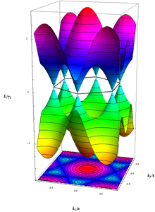
Energy of the electrons with wavenumber k in graphene, calculated in the Tight Binding-approximation. The unoccupied (occupied) states, colored in blue-red (yellow-green), touch each other without energy gap exactly at the above-mentioned six k-vectors.
The most ambitious biological application of graphene is for rapid, inexpensive electronic DNA sequencing. Integration of graphene (thickness of 0.34 nm) layers as nanoelectrodes into a nanopore[162] can solve one of the bottleneck issues of nanopore-based single-molecule DNA sequencing.

Anti-bacterial


The Chinese Academy of Sciences has found that sheets of graphene oxide are highly effective at killing bacteria such as Escherichia coli. This means graphene could be useful in applications such as hygiene products or packaging that will help keep food fresh for longer periods of time.[163]

External links


Edited:

November 2011

Monday 22 November 2010

How Rockets Work

Audience: Educators
Grades: K-12


This section of the Rockets Educator Guide explains Newton's Laws of Motion, which support the basic principles of rocketry.

How Rockets Work  [372KB PDF file]

How Rockets Work is part of the Rockets Educator Guide.

Thursday 18 November 2010

Laboratorium Astrofisika

Astrophysics Laboratory
 

  “Life is either a daring adventure or nothing.”

"Hidup adalah petualangan yang membutuhkan keberanian, bila tidak itu bukanlah hidup."


Harvard-Smithsonian Center for Astrophysics
60 Garden Street, Cambridge, MA 02138

H-R Diagram of M67 using the Clay Telescope
 
 
Instructors: Allyson Bieryla and Jonathan Grindlay
The Clay Telescope is located on the roof of the Science Center. It is a 16" telescope equipped with a CCD (charged coupled device) imager. This project is divided into three main parts. First you will learn to use the telescope to observe and image the open cluster M67 in B and V filters. We will probably need no more than three nights of observing to accomplish this, but that is just an estimate. We will then learn how to process the images using IRAF (Image Reduction and Analysis Facility) software. 

This software will enable us the tools to reduce the data, subtracting away the inherent biases of observing. We will also use IRAF to do the actual photometry to determine the magnitudes of the stars in the cluster in both B and V fields. Finally we will create an Hertzsprung-Russell diagram, which plots the V magnitude vs. B-V magnitude. This shows where the stars in the cluster are on the main sequence. From this diagram, we can estimate the cluster's age and determine the approximate distance to the cluster. Also, knowing the angular width of the CCD image and the distance to cluster, we can approximate the number of stars in a single image to get a rough density of stars in the cluster. 

Laboratory Astrophysics
Science is successful because the physical laws we discover on Earth work everywhere and every when. We use laboratory experiments to expand our understanding of physical processes and then apply these results to the processes throughout the Universe. In some cases laboratory experiments can reproduce similar physics. For example, highly charged plasmas can be created in the laboratory to study the collisions between electrons and ions that occur in the hot solar corona. In other cases, such as in the extreme environments of black holes, we cannot reproduce the conditions. However, even in those cases, the pattern of observed spectral signatures allows us to identify the species and determine some of the physical conditions and processes. Spectral features observed in the solar corona are also observed from black hole sources.  

Useful Link
 

Sunday 14 November 2010

COSMIC RAY ACCELERATION AT BLAST WAVES FROM TYPE Ia SUPERNOVAE

By: HYESUNG KANG

Department of Earth Sciences, Pusan National University, Pusan 609 -735, Korea

E-mail: hskang@pusan.ac.kr

(Received November 10, 2006; Accepted December 6, 2006)

ABSTRACT

We have calculated the cosmic ray (CR) acceleration at young remnants from Type Ia supernovae expanding into a uniform interstellar medium (ISM). Adopting quasi-parallel magnetic fields, gasdynamic equations and the diffusion convection equation for the particle distribution function are solved in a comoving spherical grid which expands with the shock. Bohm-type diffusion due to self-excited Alfv´en waves, drift and dissipation of these waves in the precursor and thermal leakage injection were included. With magnetic fields amplified by the CR streaming instability, the particle energy can reach up to 10 16 Z eV at young supernova remnants (SNRs) of several thousand years old. The fraction of the explosion energy transferred to the CR component asymptotes to 40-50 % by that time. For a typical SNR in a warm ISM, the accelerated CR energy spectrum should exhibit a concave curvature with the power-law slope flattening from 2 to 1.6 at E > ∼ 0.1 TeV. Key Words : cosmic ray acceleration – supernova remnants – hydrodynamics – methods:numerical

http://arxiv.org/pdf/astro-ph/0701027.pdf

Thursday 11 November 2010

Nobel Prize in Physics 2010

Andre Geim
Konstantin Novoselov

Konstantin Novoselov

The Nobel Prize in Physics 2010 was awarded jointly to Andre Geim and Konstantin Novoselov
 
"for groundbreaking experiments regarding the two-dimensional material graphene"

The Royal Swedish Academy of Sciences has decided to award the Nobel Prize in Physics for 2010 to

Andre Geim
University of Manchester, UK
and
Konstantin Novoselov
University of Manchester, UK
"for groundbreaking experiments regarding the two-dimensional material graphene"


Graphene – the perfect atomic lattice

A thin flake of ordinary carbon, just one atom thick, lies behind this year’s Nobel Prize in Physics. Andre Geim and Konstantin Novoselov have shown that carbon in such a flat form has exceptional properties that originate from the remarkable world of quantum physics.

Graphene is a form of carbon. As a material it is completely new – not only the thinnest ever but also the strongest. As a conductor of electricity it performs as well as copper. As a conductor of heat it outperforms all other known materials. It is almost completely transparent, yet so dense that not even helium, the smallest gas atom, can pass through it. Carbon, the basis of all known life on earth, has surprised us once again.

Geim and Novoselov extracted the graphene from a piece of graphite such as is found in ordinary pencils.

Using regular adhesive tape they managed to obtain a flake of carbon with a thickness of just one atom. This at a time when many believed it was impossible for such thin crystalline materials to be stable.

However, with graphene, physicists can now study a new class of two-dimensional materials with unique properties. Graphene makes experiments possible that give new twists to the phenomena in quantum physics. Also a vast variety of practical applications now appear possible including the creation of new materials and the manufacture of innovative electronics. Graphene transistors are predicted to be substantially faster than today’s silicon transistors and result in more efficient computers.

Since it is practically transparent and a good conductor, graphene is suitable for producing transparent touch screens, light panels, and maybe even solar cells.

When mixed into plastics, graphene can turn them into conductors of electricity while making them more heat resistant and mechanically robust. This resilience can be utilised in new super strong materials, which are also thin, elastic and lightweight. In the future, satellites, airplanes, and cars could be manufactured out of the new composite materials.

This year’s Laureates have been working together for a long time now. Konstantin Novoselov, 36, first worked with Andre Geim, 51, as a PhD-student in the Netherlands. He subsequently followed Geim to the United Kingdom. Both of them originally studied and began their careers as physicists in Russia. Now they are both professors at the University of Manchester.

Playfulness is one of their hallmarks, one always learns something in the process and, who knows, you may even hit the jackpot. Like now when they, with graphene, write themselves into the annals of science. 

Read more about this year's prize
Information for the Public
Scientific Background
Pdf 1 MB
In order to read the text you need Acrobat Reader.
Links and Further Reading


Andre Geim, Dutch citizen. Born 1958 in Sochi, Russia. Ph.D. 1987 from Institute of Solid State Physics, Russian Academy of Sciences, Chernogolovka, Russia. Director of Manchester Centre for Meso-science & Nanotechnology, Langworthy Professor of Physics and Royal Society 2010 Anniversary Research Professor, University of Manchester, UK.
www.condmat.physics.manchester.ac.uk/people/academic/geim

Konstantin Novoselov, British and Russian citizen. Born 1974 in Nizhny Tagil, Russia. Ph.D. 2004 from Radboud University Nijmegen, The Netherlands. Professor and Royal Society Research Fellow, University of Manchester, UK.
www.condmat.physics.manchester.ac.uk/people/academic/novoselov

Prize amount: SEK 10 million to be shared equally between the Nobel Laureates.

Sunday 7 November 2010

Optika Kuantum

Elektrodinamika Kuantum yang berhasil "dibersihkan" dari problem inherennya oleh Tomonaga, Schwinger, dan Feynman, mayoritas hanya dibahas pada proses-proses hamburan fisika partikel berenergi tinggi. Dapat dimaklumi bahwa pada saat itu, pun hingga sekarang, fisika partikel energi tinggi sangat menantang dan menjanjikan fenomena baru dalam fisika. Konflik antara teori Maxwell dan teori Planck saat itu dianggap tidak akan memiliki efek signifikan dalam fisika optik. Namun hal ini tidak berlangsung lama. Pada tahun 1956 dua astronomiwan, Robert Hanbury Brown dan Richard Q. Twiss, memublikasikan hasil eksperimen mereka dalam sebuah paper yang berjudul A test of a new type of stellar interferometer on Sirius pada majalah Nature. 

Pada percobaan ini dua buah detektor yang terpisah sejauh 6 meter diarahkan pada bintang Sirius. Kedua detektor tersebut menghasilkan arus elektron (listrik) dan dihubungkan dengan peralatan yang mencatat korelasinya. Diluar dugaan, kedua ilmuwan ini menemukan bahwa keluaran kedua detektor memiliki korelasi meski keduanya diletakkan pada posisi yang berlainan. Hasil eksperimen ini menimbulkan perdebatan serius dalam komunitas fisika karena dianggap tidak konsisten dengan termodinamika dan menyalahi ketidak-pastian Heisenberg. 

Hanbury Brown dan Twiss menyelesaikan masalah ini dengan menganggap bahwa foton dari dua berkas cahaya koheren yang datang dari Sirius berkorelasi. Korelasi ini selanjutnya ditransfer pada saat proses emisi fotolistrik dalam detektor. Dengan demikian foton secara individu terdeteksi dalam dunia optik! Pada tahun yang sama Edward M. Purcell menunjukkan bahwa hasil eksperimen tersebut masih memiliki interpretasi klasik, namun ia masih mengasumsikan bahwa efek tersebut merupakan indikasi sifat kuantum dari cahaya. Penemuan serta penjelasan korelasi antara dua berkas cahaya koheren ini merupakan pemicu perhatian ilmuwan pada efek kuantum yang dapat diobservasi secara optis. 

Hal ini juga diperkuat oleh penemuan laser pada tahun 1960 yang melengkapi para ilmuwan dengan sumber cahaya koheren yang sangat berbeda jika dibandingkan dengan sumber cahaya termal. Eksperimen-eksperimen selanjutnya hanya menyibak kegagalan pendekatan semi-klasik yang dijelaskan di atas. Teori yang benar baru muncul pada tahun 1963. Pada tahun 1963 Roy Glauber menghadirkan dasar-dasar teorinya pada sebuah paper singkat yang dipublikasikan dalam jurnal Physical Review Letters. Detail dari teori tersebut ia jelaskan dalam dua paper panjang berikutnya yang dipublikasi pada tahun yang sama dalam jurnal Physical Review. 

Dalam teori ini Glauber menyatakan bahwa penjelasan eksperimen korelasi foton harus berlandaskan pada aplikasi konsisten dari Elektrodinamika Kuantum. Glauber memperkenalkan konsep kuasi-distribusi dalam Optika Kuantum yang merupakan penggambaran kuantum dari satu keadaan, namun memiliki hubungan langsung dengan distribusi ruang fase klasik. Meski demikian, konsep ini menghadirkan juga sifat non-klasik, misalnya peluang distribusinya tidak positif. Jika distribusi positif, maka kita dapat memberikan interpretasi klasik. 

Glauber memperlihatkan bahwa sumber cahaya termal berhubungan dengan distribusi Gaussian sehingga teori fluktuasi dapat digunakan untuk sumber jenis ini. Kasus laser ideal tidak memperlihatkan korelasi Hanbury Brown dan Twiss. Dalam papernya, Glauber menjelaskan analisis dari formalisme untuk pendeteksian foton yang berdasarkan fungsi korelasi normal yang kini dikenal sebagai fungsi-P atau representasi Glauber-Sudarshan. Glauber mencatat bahwa statistik absorpsi foton untuk sebuah laser tidak dapat dijelaskan dengan sifat stokastik sederhana, Gaussian atau Poissonian, namun membutuhkan informasi detail keadaan kuantum dari peralatan. Keadaan-keadaan koheren ini direpresentasikan oleh osilator harmonis. Metode ini juga cocok untuk penjelasan sinyal klasik, karena osilator tersebut memiliki amplitudo dan fase. 

Dengan demikian baik efek klasik maupun fluktuasi kuantum dapat muncul secara simultan. Dalam limit intensitas cahaya yang sangat rendah jumlah foton akan sangat sedikit, sehingga efek kuantum akan dominan. Keadaan ini dapat digunakan untuk komunikasi kuantum dengan tingkat keamanan tinggi, komputasi kuantum, serta untuk merekam sinyal-sinyal super lemah pada eksperimen dengan ketelitian tinggi. Aplikasi lain dari Optika Kuantum adalah dalam penelitian aspek fundamental mekanika kuantum. Bukan rahasia lagi jika interpretasi mekanika kuantum belum dapat disepakati semua fisikawan.

 Dengan demikian kemungkinan menguji teori ini pada daerah kuantum dengan menggunakan Optika Kuantum sudah terbuka. Masih banyak aplikasi Optika Kuantum yang tidak dapat dijelaskan pada tulisan ini. Tidak dapat disangkal, jasa Glauber sudah sepatutnya dihargai dengan hadiah Nobel. 

Sumber: Dr. Terry Mart


Friday 5 November 2010

Learning and coding in biological neural networks

FIETE, ILA RANI, B.S. (University of Michigan) 1997. (Harvard University) 2000.
http://www.physics.harvard.edu/Thesespdfs/Fiete.pdf

Monday 1 November 2010

Solid-state Eelectronics

Solid-state electronics are those circuits or devices built entirely from solid materials and in which the electrons, or other charge carriers, are confined entirely within the solid material. The term is often used to contrast with the earlier technologies of vacuum and gas-discharge tube devices and it is also conventional to exclude electro-mechanical devices (relays, switches, hard drives and other devices with moving parts) from the term solid state.

While solid-state can include crystalline, polycrystalline and amorphous solids and refer to electrical conductors, insulators and semiconductors, the building material is most often a crystalline semiconductor. 

Common solid-state devices include transistors, microprocessor chips, and DRAM. DRAM devices are used in computers, flash drives and more recently, solid state drives to replace mechanically rotating magnetic disc hard drives. A considerable amount of electromagnetic and quantum-mechanical action takes place within the device. The expression became prevalent in the 1950s and the 1960s, during the transition from vacuum tube technology to semiconductor diodes and transistors. More recently, the integrated circuit (IC), the light-emitting diode (LED), and the liquid-crystal display (LCD) have evolved as further examples of solid-state devices.

In a solid-state component, the current is confined to solid elements and compounds engineered specifically to switch and amplify it. Current flow can be understood in two forms: as negatively-charged electrons, and as positively-charged electron deficiencies called holes.

The first solid-state device was the "cat's whisker" detector, first used in 1930s radio receivers. A whisker-like wire is placed lightly in contact with a solid crystal (such as a germanium crystal) in order to detect a radio signal by the contact junction effect.[6] The solid-state device came into its own with the invention of the transistor in 1947.